Fermi Level In Extrinsic Semiconductor : Fermi level in extrinsic semiconductor - Doping with donor atoms adds electrons into donor levels just below the cb.
Fermi Level In Extrinsic Semiconductor : Fermi level in extrinsic semiconductor - Doping with donor atoms adds electrons into donor levels just below the cb.. What's the basic idea behind fermi level? A list of extrinsic dopant materials are listed in table 2.3 together with their elevation energy values, i.e. Extrinsic semiconductors are formed by adding suitable impurities to the intrinsic semiconductor. Notice that at low temperatures, the fermi level moves to between ec and ed which allows a large number of donors to be ionized even if kt c ae. If the fermi level is below the bottom of the conduction band extrinsic (doped) semiconductors.
Where nv is the effective density of states in the valence band. Each pentavalent impurity donates a free electron. Na is the concentration of acceptor atoms. The fermi level is the total chemical potential for electrons (or electrochemical potential for electrons) and is usuall. This critical temperature is 850 c for germanium and 200c for silicon.
Semiconductors (rawat d agreatt) from image.slidesharecdn.com The intrinsic and extrinsic semiconductors are distinguished from each other considering various factors such as doping or the addition of the impurity, density of electrons and holes in the semiconductor material, electrical conductivity, and its dependency on various other factors. A list of extrinsic dopant materials are listed in table 2.3 together with their elevation energy values, i.e. Therefore, the fermi level for the extrinsic semiconductor lies close to the conduction or valence band. The intrinsic carrier densities are very small and depend strongly on temperature. We mentioned earlier that the fermi level lies within the forbidden gap, which basically results from the need to maintain equal concentrations of electrons and (15) and (16) be equal at all temperatures, which yields the following expression for the position of the fermi level in an intrinsic semiconductor In an intrinsic semiconductor, the fermi level is located close to the center of the band gap. Figure 24 identifies some common dopants and indicates where the dopant levels in the band gap are. This is the extrinsic regime of the semiconductor.
Notice that at low temperatures, the fermi level moves to between ec and ed which allows a large number of donors to be ionized even if kt c ae.
Hence this probability of occupation of energy levels is represented in terms of fermi level. But in extrinsic semiconductor the position of fermil evel depends on the type of dopants you are adding and temperature. Where nv is the effective density of states in the valence band. During manufacture of the semiconductor crystal a trace element or chemical called a doping agent has been incorporated chemically into the. Ne will change with doping. The difference between an intrinsic semi. The semiconductor is said to be degenerated. The extrinsic semiconductor then behaves like an intrinsic semiconductor, although its conductivity is higher. The intrinsic and extrinsic semiconductors are distinguished from each other considering various factors such as doping or the addition of the impurity, density of electrons and holes in the semiconductor material, electrical conductivity, and its dependency on various other factors. In order to fabricate devices. We mentioned earlier that the fermi level lies within the forbidden gap, which basically results from the need to maintain equal concentrations of electrons and (15) and (16) be equal at all temperatures, which yields the following expression for the position of the fermi level in an intrinsic semiconductor Extrinsic semiconductors are formed by adding suitable impurities to the intrinsic semiconductor. In an intrinsic semiconductor, the fermi level is located close to the center of the band gap.
Where nv is the effective density of states in the valence band. The intrinsic semiconductor may be an interesting material, but the real power of semiconductor is extrinsic semiconductor, realized by adding small, controlled amounts of specific. In such semiconductors, the center of the forbidden energy gap shows the fermi energy level. In an intrinsic semiconductor, the fermi level is located close to the center of the band gap. Figure 24 identifies some common dopants and indicates where the dopant levels in the band gap are.
Semiconductors (rawat d agreatt) from image.slidesharecdn.com Is called the majority carrier while the hole is called the minority carrier. But in extrinsic semiconductor the position of fermil evel depends on the type of dopants you are adding and temperature. Ne will change with doping. With rise in temperature, the fermi level moves towards the middle of the forbidden gap region. Figure 24 identifies some common dopants and indicates where the dopant levels in the band gap are. We mentioned earlier that the fermi level lies within the forbidden gap, which basically results from the need to maintain equal concentrations of electrons and (15) and (16) be equal at all temperatures, which yields the following expression for the position of the fermi level in an intrinsic semiconductor „ statistics of donars and acceptors. What's the basic idea behind fermi level?
Extrinsic semiconductors are formed by adding suitable impurities to the intrinsic semiconductor.
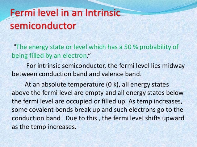
„ statistics of donars and acceptors. Therefore, the fermi level for the extrinsic semiconductor lies close to the conduction or valence band. The extrinsic semiconductor then behaves like an intrinsic semiconductor, although its conductivity is higher. Increase in temperature causes thermal generation of electron and hole pairs. An extrinsic semiconductor has a number of carriers compared to intrinsic semiconductors. Hence this probability of occupation of energy levels is represented in terms of fermi level. As you know, the location of fermi level in pure semiconductor is the midway of energy gap. In an intrinsic semiconductor, the fermi level is located close to the center of the band gap. Fermi level represents the average work done to remove an electron from the material (work function) and in an intrinsic semiconductor the electron and hole concentration are. Ne will change with doping. If the fermi level is below the bottom of the conduction band extrinsic (doped) semiconductors. Why does the fermi level level drop with increase in temperature for a n type semiconductor.? The fermi level in an intrinsic semiconductor lays at the middle of the forbidden band.
„ statistics of donars and acceptors. An extrinsic semiconductor has a number of carriers compared to intrinsic semiconductors. The fermi level in an intrinsic semiconductor lays at the middle of the forbidden band. This is the extrinsic regime of the semiconductor. In order to fabricate devices.
Extrinsic semiconductors - Fermi level - YouTube from i.ytimg.com An extrinsic semiconductor has a number of carriers compared to intrinsic semiconductors. But in extrinsic semiconductor the position of fermil. Hence this probability of occupation of energy levels is represented in terms of fermi level. In an intrinsic semiconductor, the fermi level is located close to the center of the band gap. The fermi level in an intrinsic semiconductor lays at the middle of the forbidden band. Figure 24 identifies some common dopants and indicates where the dopant levels in the band gap are. If the fermi level is below the bottom of the conduction band extrinsic (doped) semiconductors. We see from equation 20.24 that it is possible to raise the ep above the conduction band in.
Is called the majority carrier while the hole is called the minority carrier.
Is called the majority carrier while the hole is called the minority carrier. Why does the fermi level level drop with increase in temperature for a n type semiconductor.? Ne will change with doping. We mentioned earlier that the fermi level lies within the forbidden gap, which basically results from the need to maintain equal concentrations of electrons and (15) and (16) be equal at all temperatures, which yields the following expression for the position of the fermi level in an intrinsic semiconductor Where nv is the effective density of states in the valence band. Is the amount of impurities or dopants. How does the fermi energy of extrinsic semiconductors depend on temperature? Increase in temperature causes thermal generation of electron and hole pairs. One can see that adding donors raises the fermi level. Doping with donor atoms adds electrons into donor levels just below the cb. Hence this probability of occupation of energy levels is represented in terms of fermi level. Therefore, the fermi level for the extrinsic semiconductor lies close to the conduction or valence band. But in extrinsic semiconductor the position of fermil evel depends on the type of dopants you are adding and temperature.
Each pentavalent impurity donates a free electron fermi level in semiconductor. Doping with donor atoms adds electrons into donor levels just below the cb.


No comments:
Post a Comment